- Español
- Português
- русский
- Français
- 日本語
- Deutsch
- tiếng Việt
- Italiano
- Nederlands
- ภาษาไทย
- Polski
- 한국어
- Svenska
- magyar
- Malay
- বাংলা ভাষার
- Dansk
- Suomi
- हिन्दी
- Pilipino
- Türkçe
- Gaeilge
- العربية
- Indonesia
- Norsk
- تمل
- český
- ελληνικά
- український
- Javanese
- فارسی
- தமிழ்
- తెలుగు
- नेपाली
- Burmese
- български
- ລາວ
- Latine
- Қазақша
- Euskal
- Azərbaycan
- Slovenský jazyk
- Македонски
- Lietuvos
- Eesti Keel
- Română
- Slovenski
- मराठी
- Srpski језик


Products


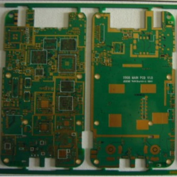
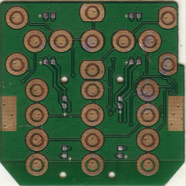
10 layer Professional circuit board fr4 electronic PCB board Multilayer PCB phone pcb
The following is about 10 layer Professional circuit board fr4 electronic PCB board Multilayer PCB phone pcb related, I hope to help you better understand A.
Send Inquiry
Product Description
10 layer Professional circuit board fr4 electronic PCB board Multilayer PCB phone pcb
if have Gerber file. please send violet(at) akesoncircuit(.) com(.) cn
Detailed Product Description
pcb board
1) Layer: 10 HDI pcb board
2) Board finished thickness: 1.0 mm
3) Material: FR-4
4) Min. drilled hole size: 0.3mm
5) Min. Line width: 4mil (0.1mm)
6) Min.Line spacing: 4mil (0.1mm)
7) Surface finish/treatment: Immersion gold
8) Copper thickness: 1 OZ
10) Solder mask color: Green
11)Inner packing: Vacuum packing / Plastic bag
Outer packing: Standard carton packing
12) Sample or mass produce, 5 to 8 days lead time
13) OEM/ODM is acceptable
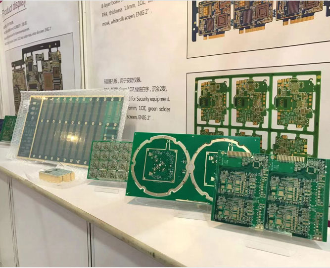
Reference - Our Production Capability for Multilayer PCB/Rigid borad
|
Item
|
M- |
|
Layer count |
1-30 layers |
|
Material |
FR4(High TG, Halogen Free, high frequency), CEM1, CEM3,BT,Al base mateiral,and so on. Supplier: SY,KB,ITEQ,Isola,Nelco,Rogers,Grance,Mitsui |
|
Maxpanel size |
32±20(800mm±508mm) |
|
Min width/space(min) |
4mil/4mil |
|
Max copper weight |
140um(4oz) for inner layer 175um(5oz) for outer layer |
|
Min machine drill size |
0.2mm(8mil) |
|
Via hole tpye |
Blind/Burried/plugged |
|
Thickness of finished board |
0.20-6.0mm |
|
Tolerance |
Registration of innerlayer to of innerlayer:±3mil Accuracy of hole position:±2mil Tolerance of dilled slot:±3mil Tolerance of PTH diameter:±3mil Tolerance of NPTH diameter:±2mil PTH hole copper thichness: 0.4-2mil Image to image tolerance:±3mil Tolerance of etching:±1mil Solder mask registration tolerance: ±2mil Finished board : Thickness<=1.0mm: +/-0.1mm Thickness>0.1mm:+/-10% Outline router: +/-0.1mm Outline Score: +/-0.2mm |
|
Color of solder mask |
Green, Black, Blue,Red, White and so on |
|
Surface freatment |
HASL,HASL Lead Free,OSP ,Immersion Gold, Immersion Ti, Immersion Sliver, Flash gold, Selective Gold plating(gold thicness up to 120u),Gold figers ,Carbon print, Peelabe Mask |
|
Hardness of solder solder |
>=6H |
|
Outline finished |
CNC, V-CUT, Punching |
|
Peel strength of line |
≥61B/in |
|
Warp and twist |
≤0.7% |


|
|
Quickly |
Sample(Normal) |
Mass(Normal) |
|
Single-sided: |
1-2 days |
3-5 days |
7-8 days |
|
Double-sided: |
2-3 days |
5-8 days |
8-10 days |
|
4 Layers: |
3-4 days |
8-10 days |
10-12 days |
|
6 Layers: |
5-6 days |
10-12 days |
12-14 days |
|
8 Layers: |
6-8 days |
10-12 days |
14-16 days |
|
10 Layers: |
8-10 days |
12-14 days |
16-18 days |
|
12 Layers: |
10 days |
14-16 days |
16-18 days |
|
>14 Layers: |
>=10 days |
>=16 days |
>=16 days |


U.S.UL product ceftification,PCB E354170 PCB;
ISO 90012008
ISO/TS 16949
QuaIity assurance standards lPC-A-600 HlPC-6011l PC-6012 BlPC-D-300 ANSl-UL-796
AnaIysis CapabiIity
In-House(Lab)
Follow the lPC-TM-650 for test function Follow the lPC-TM-650 for test function
PeeIable strength test for copper foil
Metal thickness
Flash Gold sliding pad roughness test
Solder Mask Gloss Level test
Cross section
SoIderability & Thermal shock test
Lead-free reflow simulation test(up to 280C)
Additional test can be tested at GF
authorized lab