- Español
- Português
- русский
- Français
- 日本語
- Deutsch
- tiếng Việt
- Italiano
- Nederlands
- ภาษาไทย
- Polski
- 한국어
- Svenska
- magyar
- Malay
- বাংলা ভাষার
- Dansk
- Suomi
- हिन्दी
- Pilipino
- Türkçe
- Gaeilge
- العربية
- Indonesia
- Norsk
- تمل
- český
- ελληνικά
- український
- Javanese
- فارسی
- தமிழ்
- తెలుగు
- नेपाली
- Burmese
- български
- ລາວ
- Latine
- Қазақша
- Euskal
- Azərbaycan
- Slovenský jazyk
- Македонски
- Lietuvos
- Eesti Keel
- Română
- Slovenski
- मराठी
- Srpski језик


Products
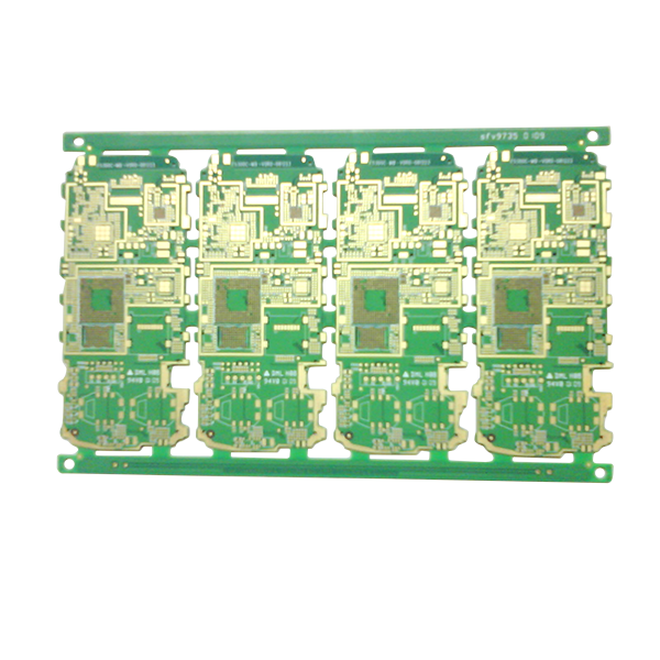
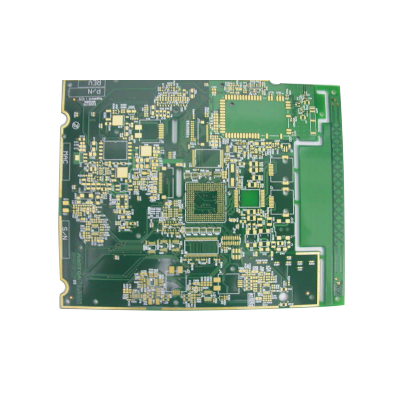
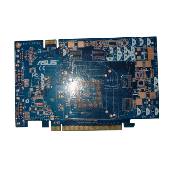

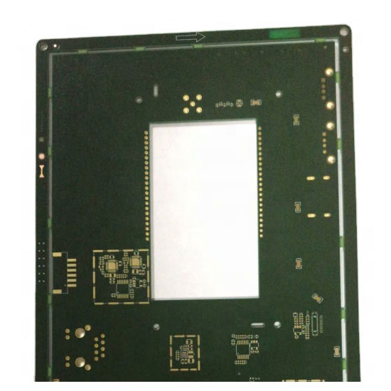
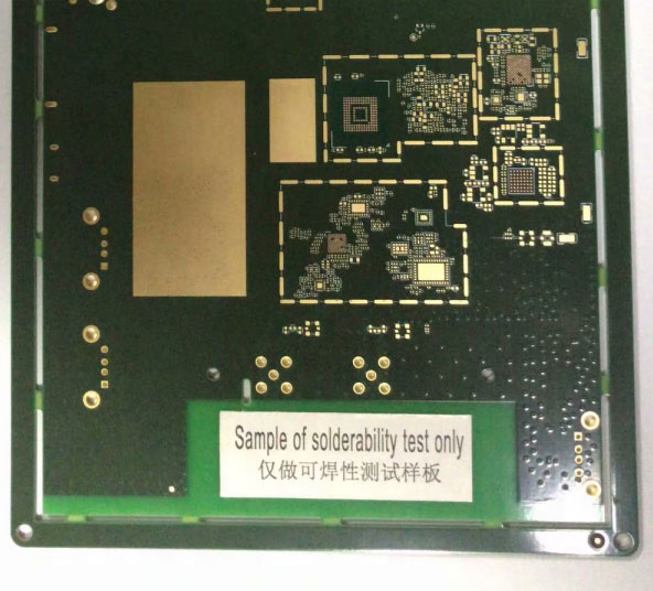
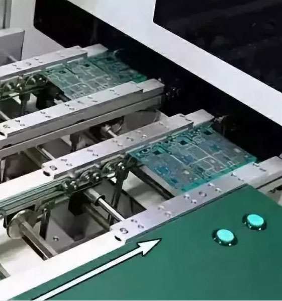
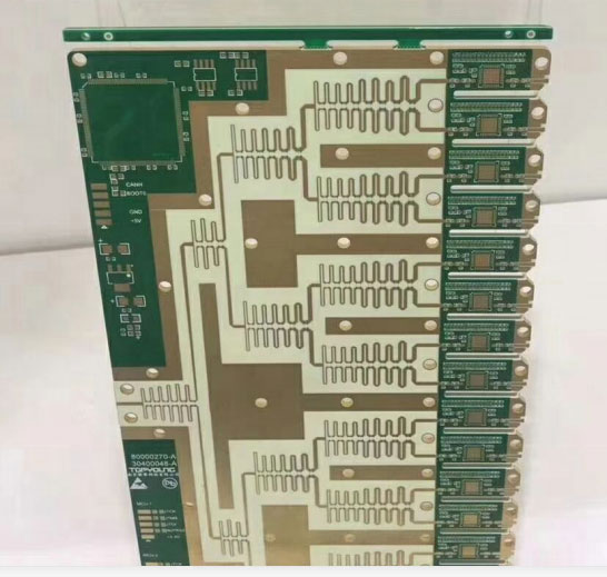
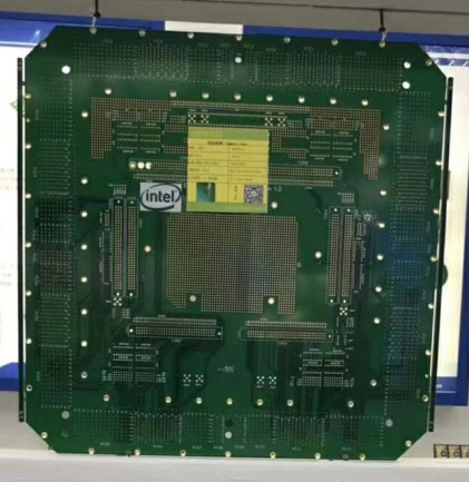
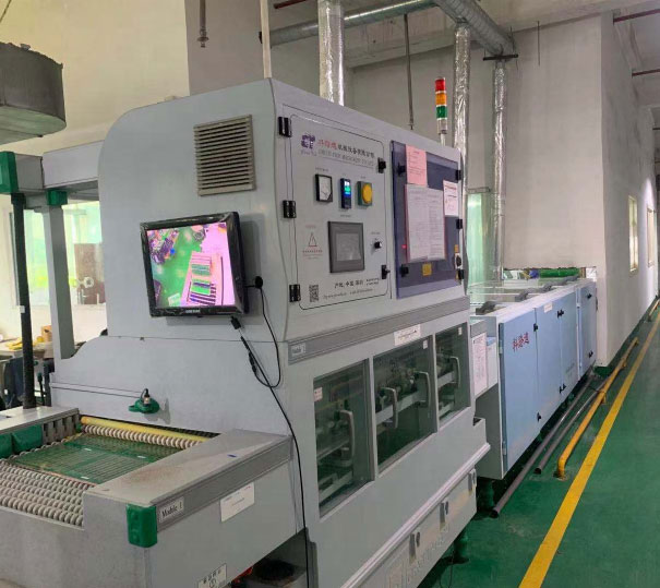
China factory Multilayer pcb 8Llayer HDI board manufacturer 3 step blind and buries board
The following is about China factory Multilayer pcb 8Llayer HDI board manufacturer 3 step blind and buries board related, I hope to help you better understand HDI PCB.
Send Inquiry
Product Description
China factory Multilayer pcb 8Llayer HDI board manufacturer 3 step blind and buries board
if have Gerbe file. please send violet(at)akesoncircuit(dot)com(dot)cn
Detailed Product Description
Multilayer pcb
1) Layer: 8 layer
2) Board finished thickness: 1.6 mm
3) Material: FR-4
4) Min. drilled hole size: 0.4mm
5) Min. Line width: 4mil (0.1mm)
6) Min.Line spacing: 4mil (0.1mm)
7) Surface finish/treatment: Immersion silver
8) Copper thickness: 1 OZ
10) Solder mask color: green
11)Inner packing: Vacuum packing / Plastic bag
Outer packing: Standard carton packing
12) Sample or mass produce, 3 to 8 days Lead time
Reference - Our Production Capability for Multilayer PCB/Rigid borad
|
Item
|
M-
|
|
Layer count
|
1-30 layers
|
|
Material
|
FR4(High TG, Halogen Free, high frequency), CEM1, CEM3,BT,Al base mateiral,and so on.
Supplier: SY,KB,ITEQ,Isola,Nelco,Rogers,Grance,Mitsui
|
|
Maxpanel size
|
32±20(800mm±508mm)
|
|
Min width/space(min)
|
4mil/4mil
|
|
Max copper weight
|
140um(4oz) for inner layer
175um(5oz) for outer layer
|
|
Min machine drill size
|
0.2mm(8mil)
|
|
Via hole tpye
|
Blind/Burried/plugged
|
|
Thickness of finished board
|
0.20-6.0mm
|
|
Tolerance
|
Registration of innerlayer to of innerlayer:±3mil
Accuracy of hole position:±2mil
Tolerance of dilled slot:±3mil
Tolerance of PTH diameter:±3mil
Tolerance of NPTH diameter:±2mil
PTH hole copper thichness: 0.4-2mil
Image to image tolerance:±3mil
Tolerance of etching:±1mil
Solder mask registration tolerance: ±2mil
Finished board : Thickness<=1.0mm: +/-0.1mm
Thickness>0.1mm:+/-10%
Outline router: +/-0.1mm
Outline Score: +/-0.2mm
|
|
Color of solder mask
|
Green, Black, Blue,Red, White and so on
|
|
Surface freatment
|
HASL,HASL Lead Free,OSP ,Immersion Gold, Immersion Ti, Immersion Sliver, Flash gold, Selective Gold plating(gold thicness up to 120u),Gold figers ,Carbon print, Peelabe Mask
|
|
Hardness of solder solder
|
>=6H
|
|
Outline finished
|
CNC, V-CUT, Punching
|
|
Peel strength of line
|
≥61B/in
|
|
Warp and twist
|
≤0.7%
|


|
|
Quickly |
Sample(Normal) |
Mass(Normal) |
|
Single-sided: |
1-2 days |
3-5 days |
7-8 days |
|
Double-sided: |
2-3 days |
5-8 days |
8-10 days |
|
4 Layers: |
3-4 days |
8-10 days |
10-12 days |
|
6 Layers: |
5-6 days |
10-12 days |
12-14 days |
|
8 Layers: |
6-8 days |
10-12 days |
14-16 days |
|
10 Layers: |
8-10 days |
12-14 days |
16-18 days |
|
12 Layers: |
10 days |
14-16 days |
16-18 days |
|
>14 Layers: |
>=10 days |
>=16 days |
>=16 days |


U.S.UL product ceftification,PCB E354170 PCB;
ISO 90012008
ISO/TS 16949
QuaIity assurance standards lPC-A-600 HlPC-6011l PC-6012 BlPC-D-300 ANSl-UL-796
AnaIysis CapabiIity
In-House(Lab)
Follow the lPC-TM-650 for test function Follow the lPC-TM-650 for test function
PeeIable strength test for copper foil
Metal thickness
Flash Gold sliding pad roughness test
Solder Mask Gloss Level test
Cross section
SoIderability & Thermal shock test
Lead-free reflow simulation test(up to 280C)
Additional test can be tested at GF
authorized lab