- Español
- Português
- русский
- Français
- 日本語
- Deutsch
- tiếng Việt
- Italiano
- Nederlands
- ภาษาไทย
- Polski
- 한국어
- Svenska
- magyar
- Malay
- বাংলা ভাষার
- Dansk
- Suomi
- हिन्दी
- Pilipino
- Türkçe
- Gaeilge
- العربية
- Indonesia
- Norsk
- تمل
- český
- ελληνικά
- український
- Javanese
- فارسی
- தமிழ்
- తెలుగు
- नेपाली
- Burmese
- български
- ລາວ
- Latine
- Қазақша
- Euskal
- Azərbaycan
- Slovenský jazyk
- Македонски
- Lietuvos
- Eesti Keel
- Română
- Slovenski
- मराठी
- Srpski језик


Products


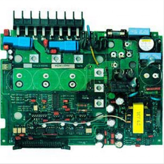
Circuit Board PCBA Servo Drive Board
The following is about Circuit Board PCBA Servo Drive Board related, I hope to help you better understand Circuit Board PCBA Servo Drive Board.
Send Inquiry
Product Description
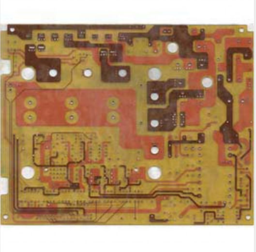
Circuit Board PCBA Servo Drive Board
Detailed Product Description:
China PCBA Assembly OEM Manufacturing Shenzhen PCBA with One Stop PCBA Service
if have Gerber file and bom list. please send violet(@)akesoncircuit.com.cn
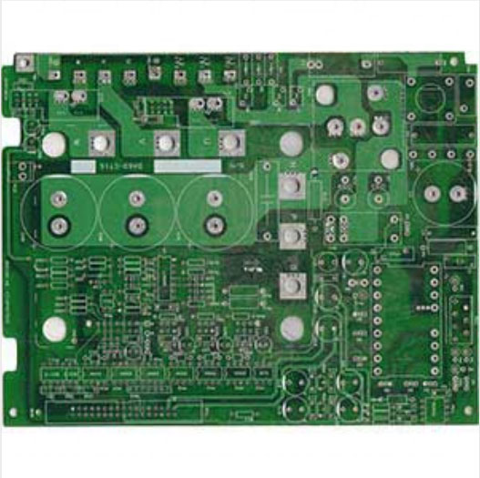
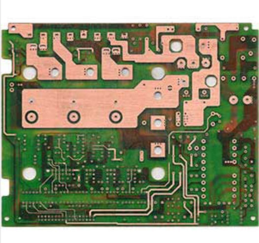
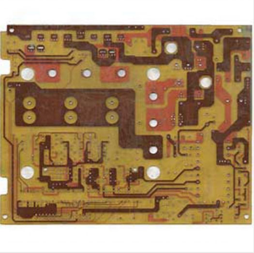
Printed circuit board
1) Layer: 4 layer
2) Board finished thickness: 1.6mm
3) Material: FR-4
4) Min. drilled hole size: 0.35mm
5) Min. Line width: 6mil (0.15mm)
6) Min.Line spacing: 6mil (0.15mm)
7) Surface finish/treatment:Immersion gold
8) Copper thickness: 1 OZ
10) Solder mask color: Black
11)Inner packing: Vacuum packing / Plastic bag
Outer packing: Standard carton packing
12) Sample or mass produce, 3 to 8 days lead time
PCBA capabilities:
• SMT assembly including BGA assembly
• Accepted SMD chips: 01005, BGA, QFP, QFN and TSOP
• Component height: 0.2-25mm
• Minimum Packing: 0201
• Minimum distance among BGA: 0.25-2.0mm
• Minimum BGA size: 0.1-0.63mm
• Minimum QFP space: 0.35mm
• Minimum assembly size: (X) 50 * (Y) 30mm
• Maximum assembly size: (X) 350 * (Y) 550mm
• Pick-placement precision: ±0.01mm
• Placement capability: 0805, 0603, 0402 and 0201
• High pin count press fit available
• SMT capacity per day: 800,000 point
Reference - Our Production Capability for Multilayer PCB/Rigid borad


|
|
Quickly |
Sample(Normal) |
Mass(Normal) |
|
Single-sided: |
1-2 days |
3-5 days |
7-8 days |
|
Double-sided: |
2-3 days |
5-8 days |
8-10 days |
|
4 Layers: |
3-4 days |
8-10 days |
10-12 days |
|
6 Layers: |
5-6 days |
10-12 days |
12-14 days |
|
8 Layers: |
6-8 days |
10-12 days |
14-16 days |
|
10 Layers: |
8-10 days |
12-14 days |
16-18 days |
|
12 Layers: |
10 days |
14-16 days |
16-18 days |
|
>14 Layers: |
>=10 days |
>=16 days |
>=16 days |


U.S.UL product ceftification,PCB E354170 PCB;
ISO 90012008
ISO/TS 16949
QuaIity assurance standards lPC-A-600 HlPC-6011l PC-6012 BlPC-D-300 ANSl-UL-796
AnaIysis CapabiIity
In-House(Lab)
Follow the lPC-TM-650 for test function Follow the lPC-TM-650 for test function
PeeIable strength test for copper foil
Metal thickness
Flash Gold sliding pad roughness test
Solder Mask Gloss Level test
Cross section
SoIderability & Thermal shock test
Lead-free reflow simulation test(up to 280C)
Additional test can be tested at GF
authorized lab