- Español
- Português
- русский
- Français
- 日本語
- Deutsch
- tiếng Việt
- Italiano
- Nederlands
- ภาษาไทย
- Polski
- 한국어
- Svenska
- magyar
- Malay
- বাংলা ভাষার
- Dansk
- Suomi
- हिन्दी
- Pilipino
- Türkçe
- Gaeilge
- العربية
- Indonesia
- Norsk
- تمل
- český
- ελληνικά
- український
- Javanese
- فارسی
- தமிழ்
- తెలుగు
- नेपाली
- Burmese
- български
- ລາວ
- Latine
- Қазақша
- Euskal
- Azərbaycan
- Slovenský jazyk
- Македонски
- Lietuvos
- Eesti Keel
- Română
- Slovenski
- मराठी
- Srpski језик


Products


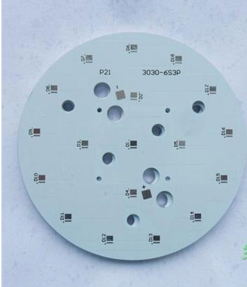

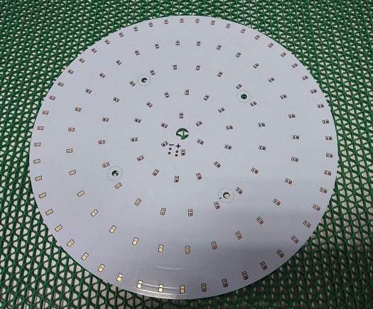
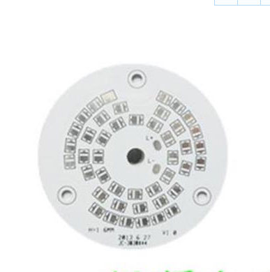
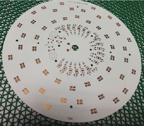
Aluminium Base PCB LED Spotlight
The following is about Aluminium Base PCB LED Spotlight related, I hope to help you better understand Aluminium Base PCB LED Spotlight.
Send Inquiry
Product Description
Aluminium Base PCB LED Spotlight
Akeson Circuit Factory 14Years Experience and more than 1000 Staffs
HASL LF HDI Buried Blind Print Circuit Board PCB (1-30layer pcb) Detailed Product Description
1) Material: FR4;2) Certificate: UL, ISO, TS16949;
3) T/T,Western Union, Paypal;
4)OEM service;
5)High quality.
Mutilayers PCB HDI Circuit Board
1. ONE-STOP-SERVICE
2. OEM service
3. Gerber file needed
4. PCB clone with sample
5. Quality guarantee and professional after-sell service
|
Item
|
Multilayers PCB High Density Circuit Board
|
|
Layer count
|
1-30 layers
|
|
Material
|
FR4(High TG, Halogen Free, high frequency), CEM1, CEM3,BT,Al base mateiral,and so on.
Supplier: SY,KB,ITEQ,Isola,Nelco,Rogers,Grance,Mitsui
|
|
Maxpanel size
|
32±20(800mm±508mm)
|
|
Min width/space(min)
|
4mil/4mil
|
|
Max copper weight
|
140um(4oz) for inner layer
175um(5oz) for outer layer
|
|
Min machine drill size
|
0.2mm(8mil)
|
|
Via hole tpye
|
Blind/Burried/plugged
|
|
Thickness of finished board
|
0.20-6.0mm
|
|
Tolerance
|
Registration of innerlayer to of innerlayer:±3mil
Accuracy of hole position:±2mil
Tolerance of dilled slot:±3mil
Tolerance of PTH diameter:±3mil
Tolerance of NPTH diameter:±2mil
PTH hole copper thichness: 0.4-2mil
Image to image tolerance:±3mil
Tolerance of etching:±1mil
Solder mask registration tolerance: ±2mil
Finished board : Thickness<=1.0mm: +/-0.1mm
Thickness>0.1mm:+/-10%
Outline router: +/-0.1mm
Outline Score: +/-0.2mm
|
|
Color of solder mask
|
Green, Black, Blue,Red, White and so on
|
|
Surface freatment
|
HASL,HASL Lead Free,OSP ,Immersion Gold, Immersion Ti, Immersion Sliver, Flash gold, Selective Gold plating(gold thicness up to 120u),Gold figers ,Carbon print, Peelabe Mask
|
|
Hardness of solder solder
|
>=6H
|
|
Outline finished
|
CNC, V-CUT, Punching
|
|
Peel strength of line
|
≥61B/in
|
|
Warp and twist
|
≤0.7%
|


|
|
Quickly |
Sample(Normal) |
Mass(Normal) |
|
Single-sided: |
1-2 days |
3-5 days |
7-8 days |
|
Double-sided: |
2-3 days |
5-8 days |
8-10 days |
|
4 Layers: |
3-4 days |
8-10 days |
10-12 days |
|
6 Layers: |
5-6 days |
10-12 days |
12-14 days |
|
8 Layers: |
6-8 days |
10-12 days |
14-16 days |
|
10 Layers: |
8-10 days |
12-14 days |
16-18 days |
|
12 Layers: |
10 days |
14-16 days |
16-18 days |
|
>14 Layers: |
>=10 days |
>=16 days |
>=16 days |


U.S.UL product ceftification,PCB E354170 PCB;
ISO 90012008
ISO/TS 16949
QuaIity assurance standards lPC-A-600 HlPC-6011l PC-6012 BlPC-D-300 ANSl-UL-796
AnaIysis CapabiIity
In-House(Lab)
Follow the lPC-TM-650 for test function Follow the lPC-TM-650 for test function
PeeIable strength test for copper foil
Metal thickness
Flash Gold sliding pad roughness test
Solder Mask Gloss Level test
Cross section
SoIderability & Thermal shock test
Lead-free reflow simulation test(up to 280C)
Additional test can be tested at GF
authorized lab