- Español
- Português
- русский
- Français
- 日本語
- Deutsch
- tiếng Việt
- Italiano
- Nederlands
- ภาษาไทย
- Polski
- 한국어
- Svenska
- magyar
- Malay
- বাংলা ভাষার
- Dansk
- Suomi
- हिन्दी
- Pilipino
- Türkçe
- Gaeilge
- العربية
- Indonesia
- Norsk
- تمل
- český
- ελληνικά
- український
- Javanese
- فارسی
- தமிழ்
- తెలుగు
- नेपाली
- Burmese
- български
- ລາວ
- Latine
- Қазақша
- Euskal
- Azərbaycan
- Slovenský jazyk
- Македонски
- Lietuvos
- Eesti Keel
- Română
- Slovenski
- मराठी
- Srpski језик


Products


Aluminum Base PCBA For Led Metal PCB
The following is about Aluminum Base PCBA For Led Metal PCB related, I hope to help you better understand Aluminum Base PCBA For Led Metal PCB.
Send Inquiry
Product Description
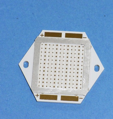
Aluminum Base PCBA For Led Metal PCB
1L/2L Al PCB
HOZ 1oz.2oz.3oz
0.6mm,0.8mm.1.0mm.1.6mm.2,0mm
HASL LF/ENG/Immersion slive/Ti
Longth LED pcb (<1.2m)
3-8days
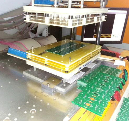
Quality system
1/Akeson has mature and stringent Q
2/100% AOI, 100% ET, 100% FQC + FQA
3/SPC and Cpk programs
4/Lean Manufacturing and 6S programs
5/Advanced inspection and lab equipment
6/Standard QA report with every shipment
7/RoHS and REACH Compliance
8/Conflict Minerals Compliance
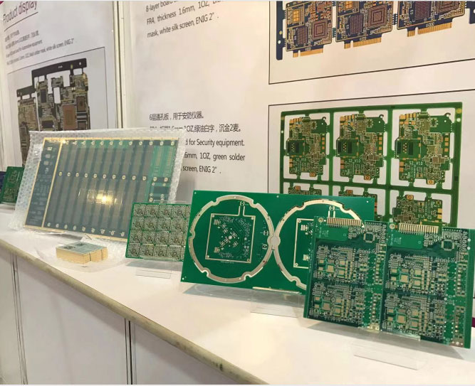
Products infomation
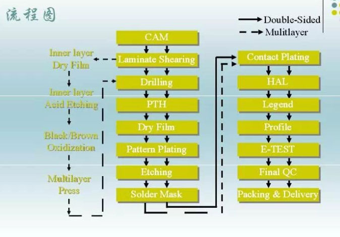
PCB Capabilities:
•Rigid PCB up to 30 layers
•Flexible PCB up to 6 layers
•Metal based PCB up to 8 layers
•Minimum drill size: 0.1mm
•Minimum line space: 0.1mm
•Minimum line width: 0.1mm
•Material used: FR4, High TG FR4, Halogen free FR4, High frequency, Ceramic, Aluminum or Copper based, Polyimide, PTFE Hybrid
•Surface finish: HAL, lead free HAL, immersion gold, silver, tin, OSP, hard gold plating, carbon ink, blue mask
•Other special technology: conductively (or non-conductively) via filling, edge plating, back drill, heavy copper (up to 10oz), Via in PAD filling, extreme large or thick PCB, Microwave & RF Circuit Boards


|
|
Quickly |
Sample(Normal) |
Mass(Normal) |
|
Single-sided: |
1-2 days |
3-5 days |
7-8 days |
|
Double-sided: |
2-3 days |
5-8 days |
8-10 days |
|
4 Layers: |
3-4 days |
8-10 days |
10-12 days |
|
6 Layers: |
5-6 days |
10-12 days |
12-14 days |
|
8 Layers: |
6-8 days |
10-12 days |
14-16 days |
|
10 Layers: |
8-10 days |
12-14 days |
16-18 days |
|
12 Layers: |
10 days |
14-16 days |
16-18 days |
|
>14 Layers: |
>=10 days |
>=16 days |
>=16 days |


U.S.UL product ceftification,PCB E354170 PCB;
ISO 90012008
ISO/TS 16949
QuaIity assurance standards lPC-A-600 HlPC-6011l PC-6012 BlPC-D-300 ANSl-UL-796
AnaIysis CapabiIity
In-House(Lab)
Follow the lPC-TM-650 for test function Follow the lPC-TM-650 for test function
PeeIable strength test for copper foil
Metal thickness
Flash Gold sliding pad roughness test
Solder Mask Gloss Level test
Cross section
SoIderability & Thermal shock test
Lead-free reflow simulation test(up to 280C)
Additional test can be tested at GF
authorized lab