- Español
- Português
- русский
- Français
- 日本語
- Deutsch
- tiếng Việt
- Italiano
- Nederlands
- ภาษาไทย
- Polski
- 한국어
- Svenska
- magyar
- Malay
- বাংলা ভাষার
- Dansk
- Suomi
- हिन्दी
- Pilipino
- Türkçe
- Gaeilge
- العربية
- Indonesia
- Norsk
- تمل
- český
- ελληνικά
- український
- Javanese
- فارسی
- தமிழ்
- తెలుగు
- नेपाली
- Burmese
- български
- ລາວ
- Latine
- Қазақша
- Euskal
- Azərbaycan
- Slovenský jazyk
- Македонски
- Lietuvos
- Eesti Keel
- Română
- Slovenski
- मराठी
- Srpski језик


Products


Power led al pcb board Al pcb for 3D printer pcb
The following is about Power led al pcb board Al pcb for 3D printer pcb related, I hope to help you better understand Power led al pcb board Al pcb for 3D printer pcb.
Send Inquiry
Product Description
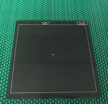
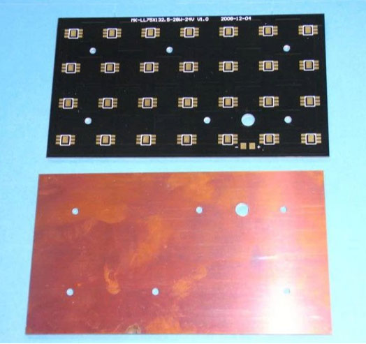
power led al pcb board Al pcb for 3D printer pcb
1) Multilayer PCBs with HDI board
2) 8Layer (1+6+1). Immersion Gold(Au;0.05um,Ni: 4um)
3) laser holes: 0.1mm. Min via: 0.2mm, line width/space:0.076/0.076mm
4) 1.0mm. FR-4 TG150 material. PP:2116/1080
5) Blue solder mask oil and wihte silkcreem
6) many BGA area control
7) Impendance control
8) Hole cooper: 0.8mil/1mil
9) Outline: Punching/CNC+CUT
9) Follow IPC 6012 class2/class3


|
|
Quickly |
Sample(Normal) |
Mass(Normal) |
|
Single-sided: |
1-2 days |
3-5 days |
7-8 days |
|
Double-sided: |
2-3 days |
5-8 days |
8-10 days |
|
4 Layers: |
3-4 days |
8-10 days |
10-12 days |
|
6 Layers: |
5-6 days |
10-12 days |
12-14 days |
|
8 Layers: |
6-8 days |
10-12 days |
14-16 days |
|
10 Layers: |
8-10 days |
12-14 days |
16-18 days |
|
12 Layers: |
10 days |
14-16 days |
16-18 days |
|
>14 Layers: |
>=10 days |
>=16 days |
>=16 days |


U.S.UL product ceftification,PCB E354170 PCB;
ISO 90012008
ISO/TS 16949
QuaIity assurance standards lPC-A-600 HlPC-6011l PC-6012 BlPC-D-300 ANSl-UL-796
AnaIysis CapabiIity
In-House(Lab)
Follow the lPC-TM-650 for test function Follow the lPC-TM-650 for test function
PeeIable strength test for copper foil
Metal thickness
Flash Gold sliding pad roughness test
Solder Mask Gloss Level test
Cross section
SoIderability & Thermal shock test
Lead-free reflow simulation test(up to 280C)
Additional test can be tested at GF
authorized lab